
A Safe 18650 LiPo Charger with a 5-12V Boost Converter
Obliczymy ostateczną cenę na podstawie wybranego pliku. Sprawdzisz ją i zaakceptujesz przed płatnością.
Zapisane na tym urządzeniu.

A panel mount drop-in carrier design for your 5-12V projects using a single 18650 LiPo battery.
- Ocena
- 0 / 5
- Polubienia
- 12
- Pobrania
- 25
- Wydruki
- 1
- Wyświetlenia
- 347
- Oceny
- 0
Aktualizacja u źródła:
Informacje o modelu
- Źródło
- Printables
- Kategoria
- Portable Devices
- Licencja
- Creative Commons — Attribution — Noncommercial — Share Alike
Do you need a portable & rechargeable 5-12V solution to power your projects? Simply add a 28-29mm (1-1/8") hole into your application & insert this power carrier design. The self-retention clips will secure it in place against a panel.
Change History
(06-07-25) 18650_lipo_charger_booster_v2. Added more clearance at PCB mounting locations to facility in-place soldering.
The following describes a charger circuit for a single-cell 18650 LiPo battery using the popular TP4056 coupled with a ME2108 or MT3608 boost converter. Understanding how each circuit works is essential when it comes to safety & extending the life of your LiPo's, not to mention saving your electronics from an unexpected failure of your power source.
IMPORTANT NOTICE: This solution is not suitable for load sharing; i.e. charging and load control at the same time. Therefore, you must disconnect any load before charging the battery when using any TP4056 based boards. With a load connected, the monitored charge current will be altered such that the current detected by the TP4056 may never terminate the battery charging process! There is a good article about the problem here: The TP4056: Lithium Ion/polymer Battery Charger IC
The good news is that you can add a load-sharing circuit yourself, or buy a different module based on something like the MCP73871. There is an excellent article on how to add load-sharing to a TP4056 board using only 3 components: TP4056 lithium charger module - modification to add power sharing - Other Hardware / General Electronics - Arduino Forum


Typical TP4056-Based Chargers
A very popular & inexpensive single-cell LiPo charger consists of the following components:
TP4056 battery charger;
DW01A one-cell LiPo Battery Protection;
FS8205 Dual N-Channel Enhancement-Mode Power MOSFET.
An important function of the DW01A is to provide over-charging & over-discharge protection, along with the use of the FS8205 to disconnect the circuit from any output electronics.
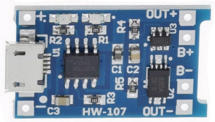

Figure 1: A typical TP4056-based PCB & Schematic
Charger Circuit Drawbacks
Although readily used, there are a number of drawbacks with respect to using most TR4056-based boards which users need to be made aware of:
Over-discharge voltage protection: The battery over-discharge voltage protection cut-off is set too low for most LiPo batteries, i.e. 2.4V. The lowest recommended working voltage for typical 18650 batteries should be around 2.75V. One solution to fix this is to add a 400 ohm resistor to ground at the VDD pin of the DW01A to act as a voltage divider with R4. This would yield an over-discharge voltage of approximately 3V vs. the 2.4V default. The disadvantage of this technique is that the resistor would create a constant current draw of approximately 8.4mA at 4.2V or 6mA at 3.0V. A better solution is to add a rectifier diode is series between R4 & VDD on the DW01A to drop the voltage down by 0.7-1.0 V;
Charge current: The charge current default is set to 1A via R3. This might be a problem for smaller batteries having lower capacities. For most LiPo's, the recommended charge rate should not exceed 1C. For example, a LiPo battery with a capacity of 500mAh should have a charge rate of no more than 500mA. Therefore, in this circuit, R3 would need to be changed to approximately 2.7K. However, for an 18650 with a 2500mAh capacity, the default 1A charge value should not be a problem;
Load Sharing: As mentioned previously, there are no load-sharing provisions available. Therefore, any load must be disconnected from the TP4056 output during charging. This is easily accomplished by having a simple switch to turn off or remove any output circuitry, like a voltage booster, from the TP4056;
Voltage booster: There is no voltage booster circuit at the output to power external electronics. Most TR4056-based boards don't contain DC-to-DC boost converters that can operate from 2.5-4.2V at the input & 5-12V @ 0.5A at the output.
IMPORTANT NOTE: The booster needs to operate down to a minimum of at least 2.5V, or at least down to the programmed minimum working voltage of the TP4056; otherwise, your boost converter could output a higher unregulated voltage & damage the output electronics.
R3 (Kohms) | I charge (mA) |
|---|---|
10 | 130 |
5 | 250 |
4 | 300 |
3 | 400 |
2 | 580 |
1.66 | 690 |
1.5 | 780 |
1.33 | 900 |
1.2 | 1000 |
Table 1: Programming Charge Current with value of R1
Alternatives to a typical TP4056 Circuit Board
There are a number of TR4056-based LiPo charger boards with integrated DC-to-DC booster ccts available. They go under product codes J5019, HW-357 & AC01, to name a few. However, the problem with most, if not all, is that they do not contain the DW01A overcharge & over-discharge protection switch OR any load sharing circuit for some odd reason & therefore, are not recommended for safe use.

Figure 2: Example of a TP4056 Board with built-in Voltage Boost Converter but with no overcharge or over-discharge protection or load-sharing circuit.
A Better Solution
So until someone develops a TP4056-based board with a boost converter AND a proper DW01A protection switch, the best & still cheapest solution is to use a separate voltage boost converter at the output of a typical TP4056 PCB. As mentioned earlier, the converter needs to operate down to the programmed over-discharge voltage protection cut-off. A good candidate is ME2108 or MT3608-based circuits, which are capable of operating at inputs down to 2.5V & therefore, compatible with TP4056-type circuits having a lower over-discharge voltage protection cut-off programmed at 2.5V or higher.

Figure 3: A typical ME2108 5V Boost Converter Schematic & PCB
ME2108 5V Boost Converter Specs
For input 2-3V: output 5V 150-380MA
For input >3V: output 5V 380-480MA
Operating frequency 150KHz, typical conversion efficiency of 85%.
Dimensions: 11mm x 10.5mm x 7.5mm
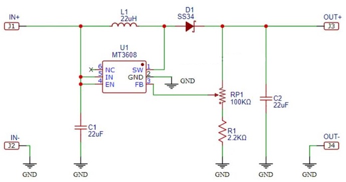
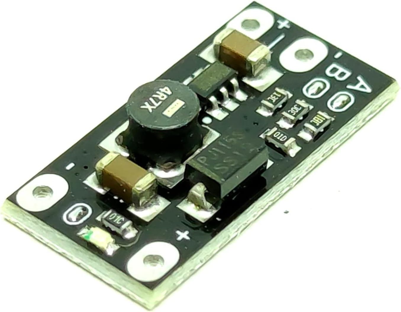
Figure 4: A MT3608 5-12V Boost Converter Schematic & PCB with jumper selection vs. potentiometer
MT3608 5-12V Boost Converter Specs
Input voltage 2.3 to 5V DC
Output Voltage 5V - 8V - 9V - 12V selectable by solder jumper or potentiometer
Maximum Output Power 6W - Maximum Output Current 1A
Operating frequency 1.2MHz, typical conversion efficiency up to 97%.
Dimensions: 11 x 22 x 4.5mm
Final Parts List
Quantity | Value / Type | Example Part # / Notes |
|---|---|---|
1 | Single-Cell Lipo Charger Board | TP4056 based |
1 | 5V Output DC to DC Booster Board | ME2108 based |
optional | 5-12V Output DC to DC Booster Board | MT3608 based |
1 | 18650 Lipo Battery Holder | Keystone Electronics P/N 1042 |