
GB Cartridge Probe Holder for Battery replacement
Obliczymy ostateczną cenę na podstawie wybranego pliku. Sprawdzisz ją i zaakceptujesz przed płatnością.
Zapisane na tym urządzeniu.

An overkilled Game-Boy Cartridge holder to keep SRAM powered during a battery replacement and thus keeping your…
- Ocena
- 0 / 5
- Polubienia
- 4
- Pobrania
- 19
- Wydruki
- 0
- Wyświetlenia
- 388
- Oceny
- 0
Aktualizacja u źródła:
Informacje o modelu
- Źródło
- Printables
- Kategoria
- Electronics
- Licencja
- Creative Commons — Attribution — Noncommercial — Share Alike
An overkilled Game-Boy Cartridge holder to keep SRAM powered during a battery replacement and thus keeping your precious saves.
Taking use of Test-Point at the back of cartridge PCB.
TP1 : RawPower -> Direct connection to SRAM's +VCC
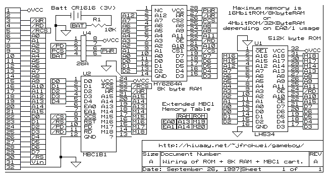
TP2 : +3V pin of Battery/GB power manager µC (ref 134A or 26A)
(TP2 is connected to TP3 via 10k Ohm resistor R1)
TP3: +3V Battery
TP4: GND
!!! WARNING: On first picture pogo pin is placed on wrong test-point. Supply +3V on TP3 will keep you SRAM powered but will damaged your already nearly depleted coin cell !!!
Minimal circuit for correct use is to supply +3V between TP1 (+VCC) and TP4 (GND), which could be achieve by soldering a CR1616 between 2 pogo.
A proper circuit would use a battery holder (there is enough room for 2 AA cell for exemple) and eventually use feedback from TP2 to shine a led to inform of correct pogo-pin contact.
Designed for 1.5mm diam pogo-pin, but it would accept any size with a little drill help.
Future improvement would be the add of something to apply pressure to the pcb to maintain it on the pogo. Ideally a clamp with a spring for easy remove.
Circuit schematics are available here thanks to Jeff Frohwein's work :
http://www.devrs.com/gb/files/hardware.html
http://www.devrs.com/gb/files/mbc1.gif
http://www.devrs.com/gb/files/134a.gif

Print instructions
Category: Electronics Summary
An overkilled Game-Boy Cartridge holder to keep SRAM powered during a battery replacement and thus keeping your precious saves.
Taking use of Test-Point at the back of cartridge PCB.
TP1 : RawPower -> Direct connection to SRAM's +VCC
TP2 : +3V pin of Battery/GB power manager µC (ref 134A or 26A)
(TP2 is connected to TP3 via 10k Ohm resistor R1)
TP3: +3V Battery
TP4: GND
!!! WARNING: On first picture pogo pin is placed on wrong test-point. Supply +3V on TP3 will keep you SRAM powered but will damaged your already nearly depleted coin cell !!!
Minimal circuit for correct use is to supply +3V between TP1 (+VCC) and TP4 (GND), which could be achieve by soldering a CR1616 between 2 pogo.
A proper circuit would use a battery holder (there is enough room for 2 AA cell for exemple) and eventually use feedback from TP2 to shine a led to inform of correct pogo-pin contact.
Designed for 1.5mm diam pogo-pin, but it would accept any size with a little drill help.
Future improvement would be the add of something to apply pressure to the pcb to maintain it on the pogo. Ideally a clamp with a spring for easy remove.
Circuit schematics are available here thanks to Jeff Frohwein's work :
http://www.devrs.com/gb/files/hardware.html
http://www.devrs.com/gb/files/mbc1.gif
http://www.devrs.com/gb/files/134a.gif
Print Settings
Printer:
i3 chinese clone
Rafts:
No
</div>Supports:No
Resolution:
0.25
</div>Infill:10%
Filament: BasicFill PLA Sylver
Notes:
Depending of your printer a brim of 2mm might be a plus to avoid any wrapping.